Floor Planning Placement And Routing In Vlsi

Pd Flow I Floorplan Physical Design Sta Synthesis Dft Automation Flow Dev Verification Services Turnkey Projects

Vlsi Design Flow Introduction To Vlsi Physical Design Floorplanning Placement Routing Nit Trichy Youtube

Edn Floorplanning Concept Challenges And Closure
Http Cc Ee Ntu Edu Tw Jhjiang Instruction Courses Spring11 Eda Lec06 2 4p Pdf
Asic System On Chip Vlsi Design Placement

Pdf Progress And Challenges In Vlsi Placement Research

A bad floor plan will lead to waste age of die area and routing congestion.
Floor planning placement and routing in vlsi. The figure depicting floor plan die size µm of samm is shown beside. Power planning is a step done along with floorplanning inorder to distribute power with proper power drop analysis across the design so that entire design is getting power uniformly. It is a factor that directly affects the following in a design. Place and route is a stage in the design of printed circuit boards integrated circuits and field programmable gate arrays as implied by the name it is composed of two steps placement and routing the first step placement involves deciding where to place all electronic components circuitry and logic elements in a generally limited amount of space.
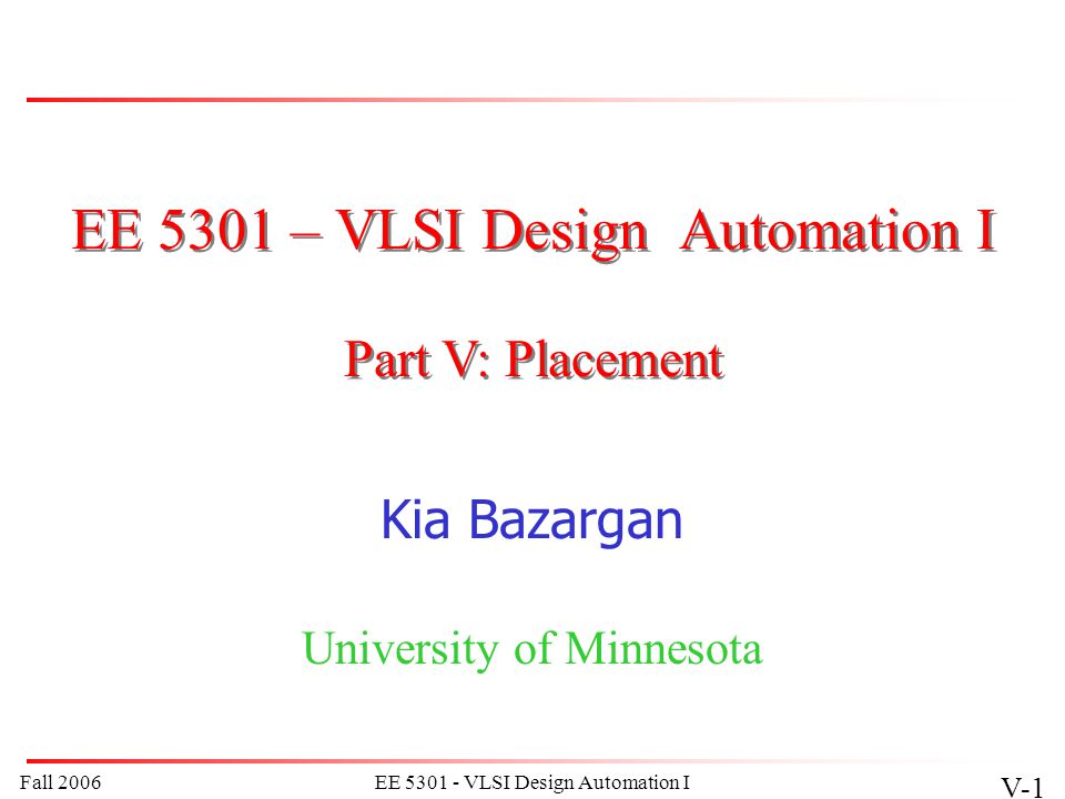
Routing placement and routing in vlsi routing in vlsi slides track assignment in vlsi routing in vlsi wiki switchbox routing in vlsi what is virtual routing in vlsi g cell in vlsi. Astro particularly uses the i o definitions from the tdf file in the starting phase of the design flow. Avoid criss cross placement of macros in order to save routing resources as well as from routing placement and congestion issues. Floorplanning is the most important stage in physical design.
Floor planning guide lines. Floor planning also decides the io structure aspect ratio of the design. Vlsichip is offering world class industry oriented vlsi design verification training program using cadence incisive enterprise simulator. Floor planning takes into account the macro s used in the design memory other ip cores and their placement needs the routing possibilities and also the area of the entire design.
Https Www Ijrte Org Wp Content Uploads Papers V8i1 A3367058119 Pdf

Figure 1 From Floor Plan Analysis In Vlsi Design Process Multi Agent Based Approach Semantic Scholar
Https Inst Eecs Berkeley Edu Eecs151 Sp18 Files Lab4 Asic Pdf
Https Www Ijeat Org Wp Content Uploads Papers V8i6 F8753088619 Pdf

Vlsi 13 Floor Planning Placement Tips Youtube

Pin By Ace Institute Of Technology On Computer Networking Training Computer Network Financial Aid Networking
Https Www Sciencepubco Com Index Php Ijet Article Download 9122 3111

1 Vlsi Physical Design Flow Download Scientific Diagram
Https Www Eng Auburn Edu Nelson Courses Elec5250 6250 Slides Asic 20layout 2 20 20digital 20innovus Pdf
Https Link Springer Com Content Pdf 10 1007 978 3 642 93464 3 27 Pdf

Figure 1 From Performance Evaluation And Comparison And Improvement Of Standard Cell Placement Techniques In Vlsi Design Semantic Scholar
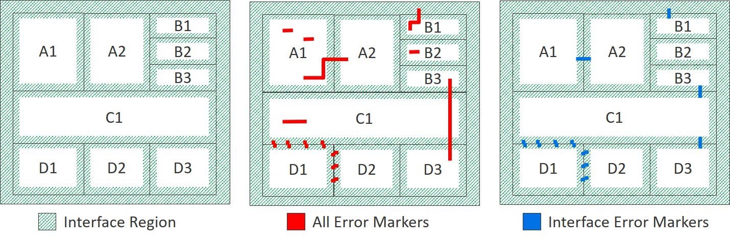
Better Manage Error Reporting At The Chip And Block Levels